
III-V Solar cells and Concentrator Arrays
Multijunction solar cells are stacks of solar cells of different materials, where each subcell is intended to absorb an convert efficiently only a fraction of the solar spectrum (a band), where photon energies are specially suited for its bandgap [1]. In this way the solar spectrum is partitioned into a number of spectrally limited bands –ideally monochromatic– which are subsequently transformed into electricity by the same number of solar cells each of them with a bandgap energy matched to that of the associated band (see Figure 1). As a result of this operating principle, in the multijunction architecture thermalization and below bandgap absorption losses are minimized and the limiting efficiency for these devices reaches 86.8% for an ideal device with an infinite number of pn junctions [2]. Multijunction solar cells with much lower number of junctions can reach remarkably high efficiencies too (as indicated by Figure 2 some limits under concentrated light are: 3J→63.8%; 4J→68.7%; 5J →72.0%, etc.) [2].
There are several material “families” that can be used to implement multijunction solar cells. However, III-V compound semiconductors (see Figure 3) provide the best palette of high quality materials for these devices and, accordingly, III-V multijunction devices have been holding the monopoly for record breaking solar cells over the past two decades [3]. For instance, dual-junction GaInP/GaAs solar cells were the first photovoltaic devices to produce conversion efficiencies over 30% in the 1990s [4]. Over the last decade, the industry standard has been a triple junction GaInP/Ga(In)As/Ge solar cell, which produces conversion efficiencies in the range of 40% [1].
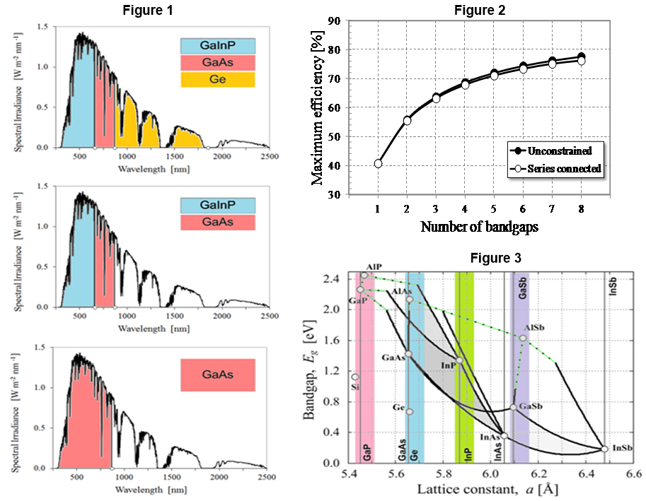
Figure 1: (left) Examples of how spectrum is used by different solar cells: (bottom) Single junction GaAs solar cell; (center) Dual-junction GaInP/GaAs solar cell; (top) Triple-junction GaInP/Ga(In)As/Ge solar cell
Figure 2 (top right) Efficiency of an ideal multi-junction solar cell as a function of the number of bandgaps under AM1.5D spectrum. Solid circles correspond to independently connected subcells while empty circles correspond to series connected (i.e. current matched) devices.
Figure 3 (bottom right) Lattice constant vs.bandgap dependence for the most common III-Vsemiconductor binary materials used in solar cells. Vertical stripes indicate compatible families for near-lattice matched designs.
As of today, the race for higher efficiencies –i.e. higher number of junctions– is ongoing and therefore there is an active quest in the PV research community for new materials to be incorporated into multijunction solar cells as fourth or even fifth junctions to further increase the efficiency of these devices. Nevertheless, the integration of a fourth junction in the well-proved GaInP/Ga(In)As/Ge design has been elusive. The use of lattice-matched materials dilute nitrides has only been successful in triple junction architectures [5]. So other alternatives are being pursued such as inverted metamorphic growth [6] or wafer bonded solar cells [7]. Both this technologies have demonstrated laboratory cells with conversion efficiencies in excess of 45%.
However, despite the fact that III-V multijunction solar cells are robust, reliable and highly efficient photovoltaic devices s, the need of expensive III-V materials has precluded their use in conventional flat-plate photovoltaics. Instead, these devices have been extensively used in high-end markets such as space applications or in less material intensive photovoltaic systems such as concentrator photovoltaics.
Published by Ignacio Rey-Stolle
References
[1] Concentrator Multijunction Solar Cells, Ignacio Rey-Stolle, Jerry M Olson, Carlos Algora, Chapter 2 of Handbook of Concentrator Photovoltaic Technology, Ignacio Rey-Stolle and Carlos Algora Eds., John Wiley and Sons Ltd. (Chichester, UK), 2016, 808 pp
[2] A. Marti and G. L. Araújo, "Limiting efficiencies for photovoltaic energy conversion in multigap systems," Solar Energy Materials and Solar Cells, vol. 43, pp. 203-222, 1996
[3] http://www.nrel.gov/ncpv/images/efficiency_chart.jpg
[4] J. M. Olson, S. R. Kurtz, A. E. Kibbler, and P. Faine, "A 27.3% efficient Ga0.5In0.5P/GaAs tandem solar cell," Appl. Phys. Lett., vol. 56, pp. 623-625, 1990
[5] D. Derkacs, R. Jones-Albertus, F. Suarez, and O. Fidaner, "Lattice-matched multijunction solar cells employing a 1eV GaInNAsSb bottom cell," Journal of Photonics for Energy, vol. 2, pp. 021805-1-021805-8, 2012.
[6] Ivan Garcia, Ryan M. France, John F. Geisz, William E. McMahon, Myles A. Steiner, Steve Johnston, and Daniel J. Friedman, "Metamorphic III–V Solar Cells: Recent Progress and Potential", IEEE Journal of Photovoltaics, Vol. 6, No. 1,pp.366-372, 2016
[7] F. Dimroth, M. Grave, P. Beutel, U. Fiedeler, C. Karcher, T. N. D. Tibbits, et al., "Wafer bonded four-junction GaInP/GaAs//GaInAsP/GaInAs concentrator solar cells with 44.7% efficiency," Progress in Photovoltaics: Research and Applications, vol. 22, pp. 277-282, 2014.


