CZTS-Kesterite
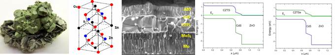
Kesterites are tetrahedrally coordinated quaternary semiconductors with general formula I2-II-IV-VI4 (I=Cu, Ag, II = Zn, Cd, Fe ; IV = Si, Ge, Sn; VI = S, Se, Te). The research on photovoltaic materials with the kesterite structure started almost 20 years ago investigating the properties of Cu2ZnSnS4 (CZTS). This compound is similar to Cu(In,Ga)Se2 (CIGS) but indium is substituted by the zinc-tin pair and selenium is replaced by sulfur. The aim was to find a semiconductor able to give high efficiency thin film solar cells without relying on any critical raw material as Indium or Gallium. The 1.5 eV direct gap of CZTS gives an high absorption coefficient over all the visible spectrum and should in principle allow to make cells with an efficiency larger than 20%. Anyway, after several years of rapid improvement, the solar cell efficiencies have leveled just below 10%: the largest efficiency value published so far is 9.2 % obtained in 2012 on a 25 cm2 minimodule by the Japanese company Solar Frontier [1].
A reason for the low efficiency, compared to 21.7% of CIGS solar cells, could be a higher band gap value, giving an unsuitable band alignment with the CdS buffer layer. A way to improve the efficiency was indeed the substitution of the sulfur with selenium. Following this approach, in 2013 IBM fabricated a 12.6% efficient solar cell [2] using Cu2ZnSn(S,Se)4 with a ratio Se:S=75:25 and a smaller gap (Eg=1.13 eV), similar to CIGS.
The factors which are currently under investigation to further improve the efficiencies are:
- interface recombination: it can be reduced by a suitable Conduction bands alignment at the buffer/kesterite interface (“spike-like”) and by creating an n-type inversion layer on the surface of the p-type kesterite absorber [3]. Several different buffer layer materials are currently under investigation to achieve these goals.
- Cation disorder: It is now well known that CZTSe has lower carrier mobility and wider band tails than CIGS, suggesting the presence of a substantial disorder level. It was also recently found that an order-disorder phase transition takes place at about 200°C [4], attributed to the ease Cu/Zn cations exchange their position in the CZTSe structure. If this is the main disorder source then the solution would be using monovalent and divalent cations less similar than Cu and Zn. Recent work on the substitution of copper with silver seems to confirm this hypothesis [5].
- band gap grading: CIGS record efficiency cells contain a band gap grading which is typically obtained by the partial substitution of In with Ga in the region near the back contact and sometimes with the partial substitution of Se with S in the region near the junction [6]. Many groups are therefore trying to include similar features in the CZTSe solar cells. Germanium seems capable to play the role of Ga in CIGS, as a substitute for Sn, since the Cu2ZnGeSe4 compound has a 1.4eV gap [7] which is a suitable enlargement of the CZTSe gap. Research on sulfur substitution on the front of the cell has just started [8] but its utility must still be assessed, especially because the effect of sulfur substitution on the band edge position is still unclear [9].
Finally we note that the development of new high efficiency cells based on “kesterites” with larger band gap could lead to tandem cells by coupling them with bottom cells of crystalline silicon or other low band-gap thin-film solar cells. Tandem cells can overcome the 33% efficiency barrier for single junction devices and allow the fabrication of devices with efficiency approaching the 40% limit.
Published by Alberto Mittiga, ENEA
References
- T. Kato, H. Hiroi, N. Sakai, S. Muraoka & H. Sugimoto. In Proc. of 27th EU-PVSEC, 2012.
- W. Wang, M.T. Winkler, O. Gunawan, T. Gokmen, T.K. Todorov, Y. Zhu & D.B. Mitzi. Adv. En. Mater., 4, 1301465 (2014).
- X. Liu, Y. Feng, F. Liu, X. Hao, G. Conibeer, D. B. Mitzi, M. Green, Progr. Photov: Res. And Appl., (2016) DOI: 10.1002/pip.2741
- G. Rey, A. Redinger, J. Sendler, T.P. Weiss, M. Thevenin, M. Guennou, B. El Adib & S. Siebentritt. Appl. Phys. Lett., 105, 112106 (2014).
- T. Gershon, Y. S. Lee, P. Antunez, R. Mankad, S. Singh, D. Bishop, O. Gunawan, M. Hopstaken, R. Haight, Adv. Energy Mater., 1502468 (2016)
- M. Nakamura, N. Yoneyama, Y. Yamaguchi, K. Sugimoto, H. Horiguchi, K. Iwata & T. Kato. In Proc. PV Specialist Conference (PVSC), 2014 IEEE 40th, page 0107 (2014).
- S. Kim, K.M. Kim, H. Tampo, H. Shibata, K. Matsubara & S. Niki. Sol.En.Mater. & Sol.Cells, 144,488 (2016).
- J. Zhong, Z. Xia, M. Luo, J. Zhao, J. Chen, L. Wang, X. Liu, D.-J. Xue, Y.-B. Cheng, H. Song & J. Tang. Sci. Reports, 4, 6288 (2014)
- D. Hironiwa, M. Murata, N. Ashida, Z. Tang & T. Minemoto. Japn. J. Appl. Phys., 53, 071201 (2014).