
cSi Wafer Based Technology
Crystalline silicon wafer technology accounted for about 93% of the total PV production in 2015 where multicrystalline silicon (multi-Si) constituted a share of 69% and monocrystalline silicon (mono-Si) a share of 24% of the total PV production [1]. Even though new cell technologies are emerging, crystalline silicon still holds stand and a majority of the solar cell production is believed to be based on crystalline silicon also in the future.
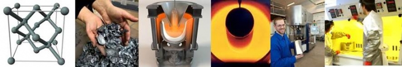
Multicrystalline silicon is made by directional solidification where heat is removed in one direction, producing a crystal with columnar microstructure where all grain boundaries run in the longitudinal direction of the ingot. Monocrystalline silicon is typically made by the Czochralski process where a single crystal is grown by carefully placing a seed in contact with the silicon melt and pulling a ingot from the melt. The solidified ingot is without grain boundaries, has a low density of dislocations and contains less metallic impurities than multicrystalline silicon. Solar modules based on monocrystalline silicon typically have an efficiency of 17% which is about 1% more (absolute) than multicrystalline modules (2015 numbers) [2]. The drawback of mono-Si compared to multi-Si is higher production costs (e.g. more labour intensive, higher energy consumption) and a higher oxygen concentration in the ingot which causes more light-induced degradation (LID). The LID effect reduces the cell performance by typically 3-7% relative [3] which constrains the capability of producing high efficiency cells.
Solidification techniques such as mono-like and high performance mc-Si have gained larger attention. Mono-like (quasi-mono) ingots are produced by directional solidification from single-crystalline seeds placed on the crucible bottom. For time being, this technology has not gained any market share. High performance mc-Si is produced either by provoking nucleation of random oriented grains at the initial stage of solidification or, more commonly, by growth from small seeds located on the crucible bottom. The produced ingots have relatively small grains, high density of random angle grain boundaries but a low density of other defects. Prognosis shows that high performance mc-Si will replace the conventional mc-Si completely [4].
Material usage for crystalline silicon cells has been reduced considerably and is now less than 6 g Si/Wp [5]. This is a result of continuous optimization efforts such as increasing cell efficiencies, higher throughput, cutting thinner wafers and a reduction of silicon losses in the wafering process (kerf loss). Large potentials lie in developing new and improved techniques to obtain wafers from the silicon ingots, such as using diamond wire saws or kerfless methods predominately based on lift-off techniques (described in more detail in Ultra-thin and Kerfless Silicon Wafer Development. Other important aspects will be to find efficient ways to recycle kerf loss and ingot cut-offs and to increase ingot yield further.
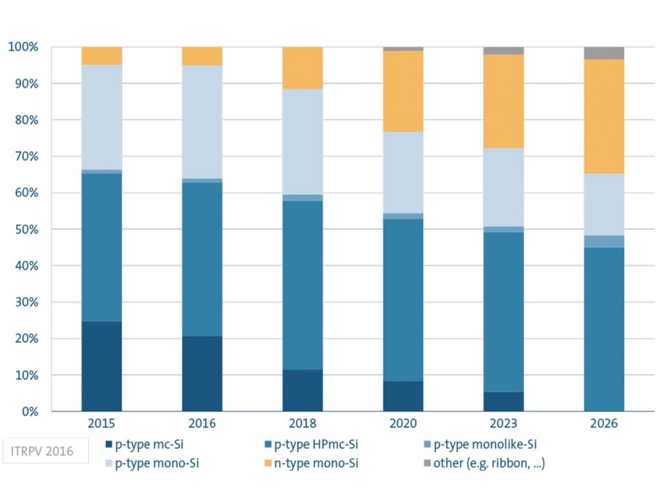
World market shares for different wafer types [4]
Cell efficiencies must be further increased in order to make PV cost competitive to other energy sources. The high quality single crystal material is believed to have a higher potential to achieve this efficiency increase compared to multi-Si. On the other hand, multi-Si has a higher scalability due to a more robust process. N-type silicon is used for advanced cell concepts demonstrating high efficiencies, such as HIT and IBC cells. N-type silicon has the advantage of supressing LID, harmfulness of impurities is reduced and the material degrades less during high temperature processing steps compared to p-type silicon. A gradual transition to n-type material is believed to take place for mono-Si [4]. However, obstacles such as a more complicated emitter process, passivation, metallization and cell edge isolation must be overcomed [6].
Cell technology will further develop and among high-efficiency products, PERC (Passivated Emitter Rear Cell) has the highest cost-performance ratios and are currently the most competitive in the industry [7]. This cell technology will increase considerably the coming years both within p-type mono- and multi-Si [8].
Considerable research and development efforts are done on cell types based on ribbon growth (RGS), conventional thin-film technology (e.g. amorphous silicon, CdTe and CIGS) and emerging thin-film technologies (e.g. organic cells, perovskite cells and dye-sensitized solar cell). However, cells based on crystalline silicon are shown to not be easily replaced. No other material has the same favourable composition of properties as silicon; abundancy, non-toxic, scalability, reliability and durability. The full potential of silicon solar cells has not been reached and as crystalline silicon will continue to be the major player in the PV market, further development of material characteristics, processes and cell concepts is important.
Published by Rannveig Kvande,SINTEF
References
[1] IHS (Mono-/Multi- Proportion from Cell Production). Graph: PSE AG 2016
[2] International Renewable Energy Agency (Irena), "The Power to Change: Solar and Wind Cost Reduction Potential to 2025", June 2016
[3] S. Sterk, K. Münzer, S. Glunz, "Investigation of the degradation of crystalline solar cells", Proc. 14th European PVSEC, 1997, p.85
[4] International Technology Roadmap for Photovoltaics (ITRPV), "2016 Results including maturity reports", 7th edition, October 2016
[5] Fraunhofer ISE: Photovoltaics Report, updated: 17th November 2016
[6] J. Libal, R. Kopecek, "N-type silicon solar cell technology: ready for take off?", www.pv-tech.org[7] EnergyTrend, "PERC shows its worth", PV magazine, issue 09/2015
[8] Bloomberg New Energy Finance, "2015 PV Market Outlook", ASEF Manila, June 2015
Infrastructure
Expertise
 CÁRABE Julio
 GORDON Ivan
 ROCA Francesco
 LA FERRARA Vera
 MORVILLO Pasquale
 MALBRANCHE Philippe
 DEL CAÑIZO Carlos
 BINETTI Simona
 REALE Andrea
 PONCE-ALCÁNTARA Salvador
 ACCIARRI Maurizio
 KODOLBAS Alp Osman
 ALAGÖZ Arif Sinan
 ØVRELID Eivind
 DALAKER Halvor
 DE WOLF Stefaan
 REBER Stefan
 DRIEßEN Marion
 BECKER Christiane
 BANSEN Roman
 FOSS Sean Erik
 MARSTEIN Erik Stensrud
 SELJ Josefine
 NORDSETH Ørnulf
 ZHU Junjie
 VAN NIEUWENHUISEN Kris
 DEPUAW Valerie
 TURAN Rasit
 DEMIRCIOGLU Olgu
 LUQUE Antonio
 STOKKAN Gaute
 RYNINGEN Birgit
 NOS AGUILA Oriol
 IZZI Massimo
 MERCALDO Lucia Vittoria
 TUCCI Mario
 LANCELLOTTI Laura
 VEIRMAN Jordi
 SCHWARK Michael
 LAGUNAS Ana Rosa
 SLAOUI Abdelilah
 SERRA João
 KVANDE Rannveig
 SIVARAMAKRISHNAN Hariharsudan
 KALOGIROU Soteris
 HAUG Halvard
 GOUTTEBROZE Sylvain
 DANEL Adrien
 ROUX Charles
 CASAJUS Luis
 BENGOECHEA Jaione
EZQUER Mikel
BENGOECHEA Jaione
EZQUER Mikel
 ZUGASTI Eugenia
 RODRÍGUEZ María Jesús
 LANG Felix