Ultra-thin and kerfless silicon wafer development
The International Technology Roadmap for Photovoltaics (ITRPV) [1] predicts a continued reduction in the silicon wafer thickness in the coming years. However, in the last 2-3 years, the predicted reduction in the wafer thickness did not happen and wafer thickness stagnated at around 180 µm. This is because further decreases in wafer thickness are quite challenging for both the wafering process and all subsequent down-stream handling steps in solar cell and module production, with increased risk of wafer breakages and hence yield loss [2, 3].
Nevertheless, it would be very beneficial for the photovoltaic industry to go to thinner silicon substrates with a thickness below 100 µm. The first reason for this is that a better silicon utilisation and the use of thinner silicon substrates without compromising on the high cell efficiencies would lead directly to a substantial cost reduction of silicon modules. This follows from the fact that the cost of silicon (which is the sum of useful silicon used in cell processing and the silicon lost in the kerf during wire sawing of silicon ingots into wafers ) constituted a significant 33% of the total cost of silicon solar modules at the beginning of 2015 [1].
A second reason supporting the reduction in the silicon thickness of solar cells is the possible increase in cell performance of thinner cells. As the silicon thickness is reduced, the volume of silicon available for recombination is also reduced. Provided excellent surface passivation can be achieved, this will result in an increase in the open-circuit voltage as the cell is made thinner. On the other hand, since silicon is an indirect bandgap semiconductor, absorption of photons is inefficient in thinner cells. Thus, a thinner cell would absorb less photons and this may result in a lower short-circuit current. However, with the design of an efficient light trapping scheme, it is possible to increase the path length of light within the cell such that this loss in short-circuit current can be minimised. Nevertheless, these opposing effects set up a trade-off between achieving high photo-generated current and high open-circuit voltage, resulting in a possible optimum thickness for silicon solar cells. It has been shown that depending on the bulk quality, the surface passivation quality, the light trapping efficiency and certain economic factors, high efficiencies at least comparable to present-day thick (180 µm) solar cells can be attained with silicon thicknesses in the range of 30-100 µm [4, 5].
A third reason for going towards ultra-thin silicon solar cells is that cells in the sub-50 µm thickness range are likely to be quite flexible and lighter in weight than the standard bulk silicon solar cells of today. Such thin and flexible solar cells can be an asset for the burgeoning field of building-integrated photovoltaics (BIPV), where solar modules are used as building materials for roofs such as roof tiles and shingles or semi-transparent facades [6, 7].
It is clear that with the present wafering technologies and the present value chain of silicon wafers as shown in Figure 1, it is impossible to achieve sub-100 µm silicon wafer thickness and to eliminate kerf loss. As a result, research has been ongoing on a variety of innovative and disruptive technologies which allow (1) the production of very thin silicon wafers or foils that are 1-2 orders of magnitude thinner than present-day wafers and (2) the elimination or minimisation of kerf loss from the silicon solar module production value chain. These kerfless ultra-thin silicon wafer production technologies are predominantly based on lift-off technologies.
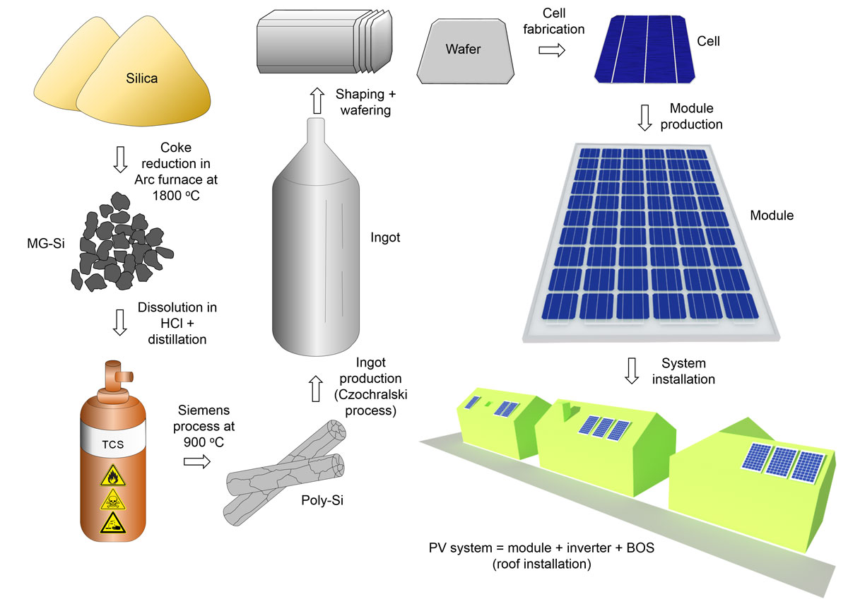
Figure 1. Monocrystalline silicon photovoltaic system value chain.
Broadly-speaking, the essence of all lift-off or layer transfer processes can be captured in four main steps in the lift-off sequence [8], even though the intricacies of each method means that they are quite different from each other and do not always follow a particular sequence. The four steps are as follows:
- Substrate modification: the parent (e.g. ingot, thick wafer, etc.) from which an ultra-thin silicon layer will be extracted is modified in the first step to condition the top of the parent for lift-off. This could be done by deposition of a sacrificial layer (surface modification), etching (near-surface modification), implantation (deep sub-surface modification), or even laser notching on the edge of the substrate or ingot (edge modification).
- Active layer definition: during this step, the actual layer to be lifted-off is defined. This could be the epitaxial deposition of the active layer itself, or the formation of a sub-surface detachment plane by annealing that delineates the layer to be lifted-off.
- Detachment of the active layer: finally, the parent sample is subjected to a process which activates the release of the active layer by breaking the physical connections between the parent and the lift-off layer. This could, for instance, be the chemical dissolution of the sacrificial layer underneath the active layer, or the mechanical crack propagation underneath the active layer parallel to the surface.
- Re-use of the parent: A typical feature of most lift-off processes is the re-using of the parent for multiple cycles of lift-off and/or layer transfer. This re-use is a prerequisite for low-cost production of the kerfless wafers.
A comprehensive overview of various kerfless wafering methods or lift-off processes is given by Henley [9], categorised according to the phase of the silicon source (i.e. solid, liquid or gas phase) used for producing the thin silicon. A similar overview on a subset of techniques is also given by Brendel [8] and McCann et al. [10]. The silicon solar value chain including the lift-off options is shown in Figure 2.
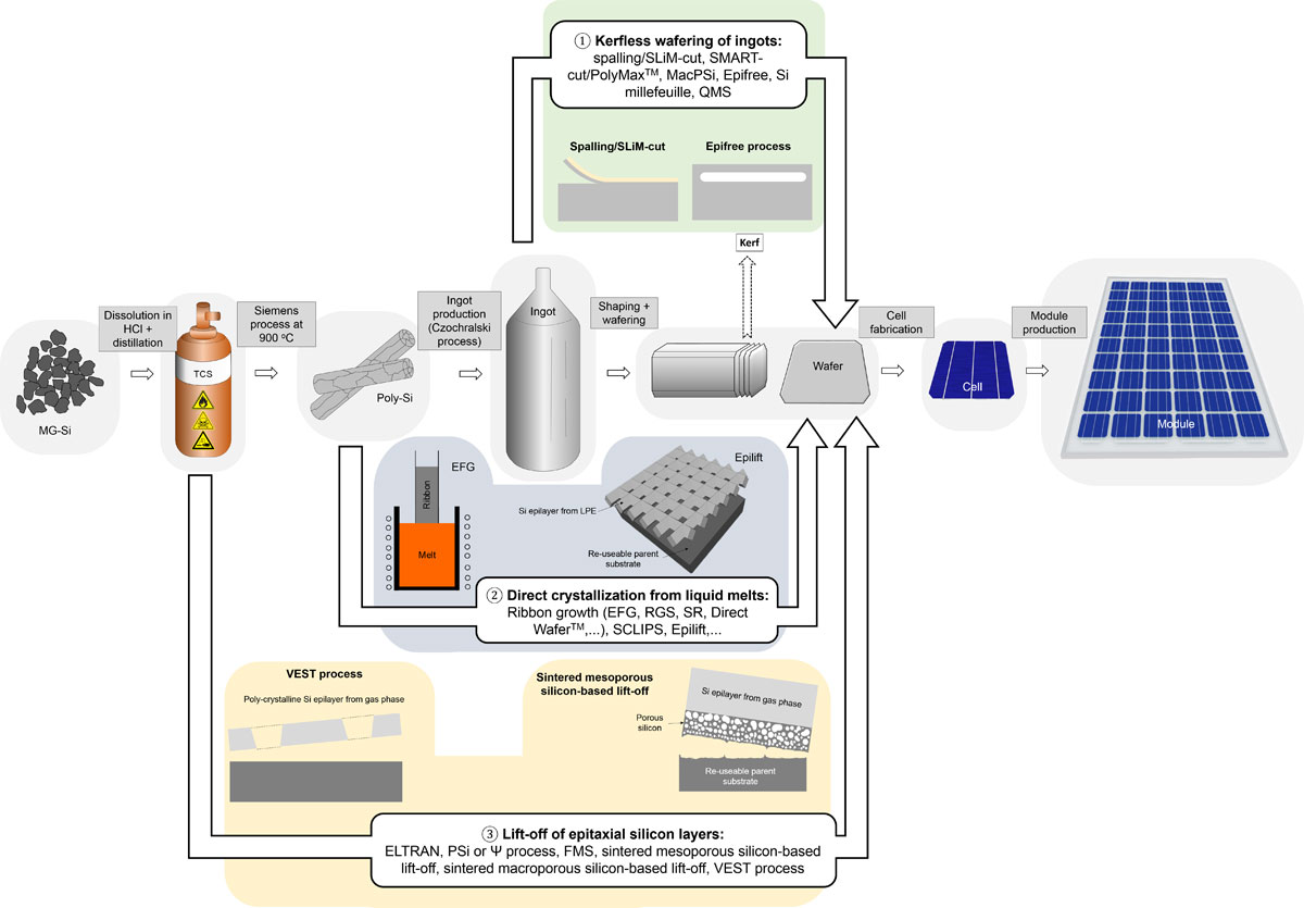
Figure 2. Si value chain with lift-off options
For conventional wafer-based c-Si PV, solar cell fabrication, cell interconnection and module encapsulation proceed sequentially one after the other. Solar cells are first fabricated from wafers, then tabs are soldered onto the cell bus bars and the cells are interconnected by stringing them together. Subsequently, the interconnected cells are encapsulated in a laminate assembly. This sequential approach taken in conventional wafer-based c-Si PV manufacturing inherently assumes the mechanical rigidity and stability of silicon wafers, and their ability to withstand the rigours of the module production sequence in a freestanding configuration. However, as the thickness of c-Si reduces, there are concerns about the mechanical yield of following the conventional route to module production. Firstly, for thin silicon produced by lift-off, there is the very high risk of breakages during cell processing due to handling, manipulating and processing that induce large stresses. Secondly, thinner silicon cells are more susceptible to mechanical yield loss during cell interconnection through breakages due to stresses arising from the soldering of ribbons in the tabber-stringers, and to failure during operation through propagation of micro-cracks formed during the interconnection processes, which could eventually reduce the reliability and the operational lifetime of solar modules [11, 12].
One solution to the problem of lack of mechanical rigidity of thin silicon is to artificially increase their rigidity during cell processing and cell interconnection by bonding the silicon either temporarily or permanently to a mechanically-strong or rigid substrate. This support can be provided by the parent substrate (before lift-off), a low-cost foreign wafer carrier (e.g. ceramics, metal foils, glass, plastics, or low-cost silicon substrates) or as in the case of thin-film PV, the module glass or the module back layer. This approach has inspired the on-going development of several novel module concepts that are positioned in between the completely sequential wafer-based c-Si PV and the completely integrated thin-film PV module manufacturing, consisting of varying degrees of integrated cell level and module level device processing.
Published by Hariharsudan Sivaramakrishnan, Valerie Depauw, and Ivan Gordon, IMEC
References:
- http://www.itrpv.net/
- K. a. Münzer, K. T. Holdermann, R. E. Schlosser, and S. Sterk, “Thin monocrystalline silicon solar cells,” IEEE Trans. Electron Devices, vol. 46, no. 10, pp. 2055–2061, 1999.
- D. Kray, H. Kampwerth, E. Schneiderlöchner, A. Grohe, F. Kamerewerd, A. Leimenstoll, D. Osswald, E. Schäffer, S. Seitz, S. Wassie, S. Glunz, and G. Willeke, “Comprehensive experimental study on the performance of very thin laser-fired high-efficiency solar cells,” in Proceedings of the 19th European Photovoltaic Solar Energy Conference, 2004, pp. 608–611.
- A. Bozzola, P. Kowalczewski, and L. C. Andreani, “Towards high efficiency thin-film crystalline silicon solar cells: The roles of light trapping and non-radiative recombinations,” J. Appl. Phys., vol. 115, no. 9, p. 094501, Mar. 2014.
- D. M. Powell, J. Hofstetter, D. P. Fenning, R. Hao, T. S. Ravi, and T. Buonassisi, “Effective lifetimes exceeding 300 μs in gettered p-type epitaxial kerfless silicon for photovoltaics,” Appl. Phys. Lett., vol. 103, no. 26, p. 263902, 2013.
- J. Yoon, A. J. Baca, S.-I. Park, P. Elvikis, J. B. Geddes, L. Li, R. H. Kim, J. Xiao, S. Wang, T.-H. Kim, M. J. Motala, B. Y. Ahn, E. B. Duoss, J. a Lewis, R. G. Nuzzo, P. M. Ferreira, Y. Huang, A. Rockett, and J. a Rogers, “Ultrathin silicon solar microcells for semitransparent, mechanically flexible and microconcentrator module designs.,” Nat. Mater., vol. 7, no. 11, pp. 907–915, 2008.
- A. W. Blakers and T. Armour, “Flexible silicon solar cells,” Sol. Energy Mater. Sol. Cells, vol. 93, no. 8, pp. 1440–1443, 2009.
- R. Brendel, “Review of layer transfer processes for crystalline thin-film silicon solar cells,” Japanese J. Appl. Physics, Part 1 Regul. Pap. Short Notes Rev. Pap., vol. 40, no. 7, pp. 4431–4439, 2001.
- F. J. Henley, “Kerf-free wafering: Technology overview and challenges for thin PV manufacturing,” Conf. Rec. IEEE Photovolt. Spec. Conf., pp. 1184–1192, 2010.
- M. J. McCann, K. R. Catchpole, K. J. Weber, and A. W. Blakers, “A review of thin-film crystalline silicon for solar cell applications. Part 1: Native substrates,” Sol. Energy Mater. Sol. Cells, vol. 68, no. 2, pp. 135–171, 2001.
- S. Pingel, Y. Zemen, and O. Frank, “Mechanical stability of solar cells within solar panels,” in Proceedings of the 24th European Photovoltaic Solar Energy Conference, 2009, pp. 3459–3463.
- A. Gabor, M. Ralli, S. Montminy, L. Alegria, C. Bordonaro, J. Woods, and L. Felton, “Soldering induced damage to thin Si solar cells and detection of cracked cells in modules,” in Proceedings of the 21st European Photovoltaic Solar Energy Conference and Exhibition, 2006, pp. 2042–2047