SINTEF-Laue scanner & Lateral Photovoltage Scanning LPS
- Measuring crystal orientation on silicon samples on industrial bricks and standard wafer sizes (156×156 mm2)
- Lateral Photovoltage Scanning (LPS) to measure locally resistivity variations in silicon sample to detect dopant striations
Technical Info
LAUE SCANNER
Laue scanner is used for measuring crystal orientation on silicon samples. It can be used for measuring on industrial bricks and standard wafer sizes (156×156 mm2) without any additional surface preparation.
 While EBSD measures grain orientation on small areas (5×5 cm2) and requires time consuming sample preparation, Laue can scan large size samples and may be used on as-cut surfaces. The first part of the measurement is constituted by visualizing the grains, requiring some contrast between the grains for a proper grain detection. Subsequently, the grain orientation is measured by X-ray diffraction in the middle of each detected grain.
The sample surface is first illuminated by LED lamps located in a circle above the sample in two heights. Due to the different locations of the lamps, the sample is illuminated at different angles which optimizes the detection of grains. The grains are detected by a visual camera located above the sample.
The software is then calculating the middle of each grain where the grain orientiation is measured by the Laue method. A white X-ray beam creates a backscatter diffraction pattern of all possible lattice plane families, due to all wavelengths being included in the white X-ray beam. The measured Laue pattern is compared to known Laue pattern for the different grain orientations to detect the grain orientation in the measured spot.
LPS - LATERAL PHOTOVOLTAGE SCANNING
During solidification of silicon, variation in growth rate occurs locally and induces small variations in dopant concentrations in the solidified ingot. This is visible as striations in a LPS image. The striations are observed both in multicrystalline and monocrystalline ingots. However, striations are most pronounced in monocrystalline silicon ingot where both thermal striations, which is a result of melt convection, and rotational striations, caused by crystal rotation off-centered from the thermal axis, occur.
When using LPS, the sample is electrically connected on opposite sides. If there are doping variations (i.e. resistivity gradients) laterally in the sample within the laser spot area, internal electric fields are created. This will create a drift of free electrons and holes along the field in opposite directions and the resu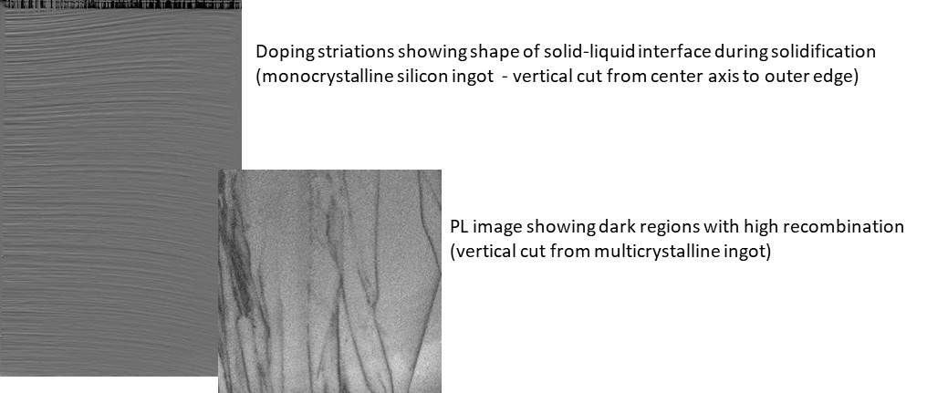 lting current is detected as a voltage drop between the two opposite contacts at the rims of the sample. The magnitude of the measured voltage depends on the lateral resistivity gradient. The technique is used to detect dopant and oxygen striations in silicon. From the striation profiles it is possible to detect the shape of the solid-liquid interface during solidification and how the interface shape changes during solidification.
In PL imaging, photolumenscence will be emitted when electron-hole pairs generated by the laser relax back to their original state (i.e. recombine). The PL intensity is measured and provides information about the silicon quality where regions with high recombination are shown as dark areas in the PL image. Dark areas are related to regions with a high defect density, typically caused by dislocations or grain boundaries decorated with impurities. The measurements are only qualitative and do not provide minority carrier lifetime values.
Striations in as-cut silicon samples are hardly visible and it is recommended that the sample surface is polished before LPS measurement. PL requires polished surface.
Main technical Features
- LAUE SCANNER: Measuring crystal orientation on silicon samples on industrial bricks and standard wafer sizes (156×156 mm2)
- LATERAL PHOTOVOLTAGE SCANNING(LPS): to measure locally resistivity variations in silicon sample to detect dopant striations
Limitations or constraints
N/D
Typical services or results
- Measurements
- Characterization
Participation to Research Projects:
N/D