UPM-Silicon production
- Semi-industrial plant for silicon purification, synthesis, crystal growth by the Czochralski method and characterization
Technical Info
Support in the development of silicon purification technologies is given, both through the chemical and the metallurgical routes. Advice is provided to assess the technology potential and the material requirements to be met. A lab-type CVD reactor for silicon deposition from trichlorosilane is used for the proof-of-concept of innovative concepts. Advanced characterization of material quality is performed to provide guidance to process optimization.
Monocrystalline ingots with non-standard characteristics are grown in an 80 kg load Czochralski puller (UMG silicon, granular silicon, alternative dopant).
MAIN TECHNICAL FEATURES:
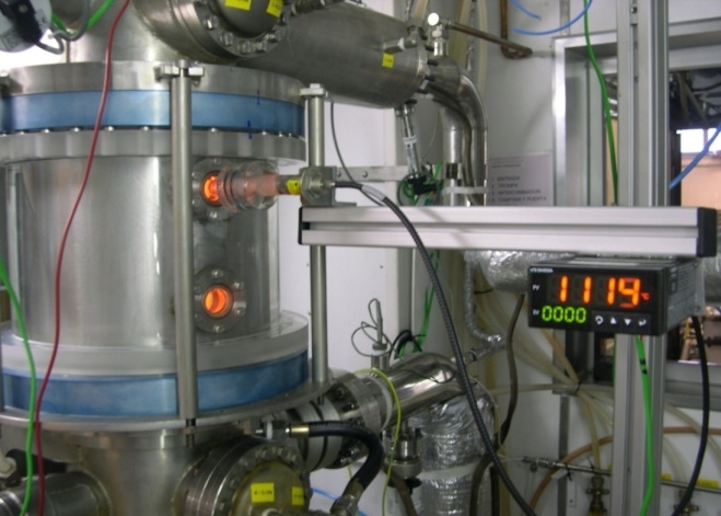
1.- Siemens-type lab reactor
- CVD reactor for polysilicon deposition from Trichlorosilane
- Deposition at 1 bar in the 1000-1100ºC range
- Typical growth rate of 2-3 μm/min in 1-10 doped seed rods
- Deposition in alternative surfaces
2.-Pilot plant for silicon purification via chlorosilanes, ∼50 t/a capacity
- Fluidized Bed Reactor for chlorosilane production from Silicon Tetrachloride
- Fix Bed Reactor for chlorosilane production from Hydrogen Chloride
- Distillation columns
- Siemens CVD reactor for 18 U-rods
- Clean room for polysilicon post-processing
3.-Monocrystalline ingot grower by the Czochralski method
- PVA TEPLA mod EKZ 2700
- 80 kg load, up to 6’’ diameter
- Growth of ingots from unconventional Si feedstock
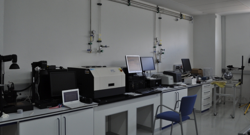
4.- Process and Material Characterization
- Mass Spectrometer
- Chromatograph
- BLS-I /BCT-400 Photoconductance Lifetime Tester for Ingots
LIMITATIONS OR CONSTRAINTS :
- The access will be allowed with technical and scientific assistance from staff of the Instituto de Energía Solar (UPM)
TYPICAL SERVICES OR RESULTS
- Proof of concept of innovative approaches for polysilicon deposition by CVD
- Growth of ingots from unconventional Si feedstock
- Characterisation of silicon materials
LIST OF SERVICES AGAINST PAYMENT:
Silicon deposition by CVD and Crystal growth services will be priced once the scope of the planned experiments is established.
Participation to Research Projects:
The infrastructure has been developed mostly thanks to fundings from the Spanish Ministerio de Ciencia e Innovación (now Ministerio de Economía y Competitividad), in the framework of “Proyectos Singulares y de Carácter Estratégico”, PSE-120000-2006-5, PSE- 120000-2007-3, PEN-120000-2009-35), and “Actuaciones científicas y tecnológicas en parques científicos y tecnológicos”, PCT-420000-2009-17. It has also been used in contracts with private companies, both national (Spanish) and international
Photo