
LPS - Lateral Photovoltage Scanning
PV Material and Device Characterization Equipment

During solidification of silicon, variation in growth rate occurs locally and induces small variations in dopant concentrations in the solidified ingot. This is visible as striations in a LPS image. The striations are observed both in multicrystalline and monocrystalline ingots. However, striations are most pronounced in monocrystalline silicon ingot where both thermal striations, which is a result of melt convection, and rotational striations, caused by crystal rotation off-centered from the thermal axis, occur.
Main Technical Features
When using LPS, the sample is electrically connected on opposite sides. If there are doping variations (i.e. resistivity gradients) laterally in the sample within the laser spot area, internal electric fields are created. This will create a drift of free electrons and holes along the field in opposite directions and the resu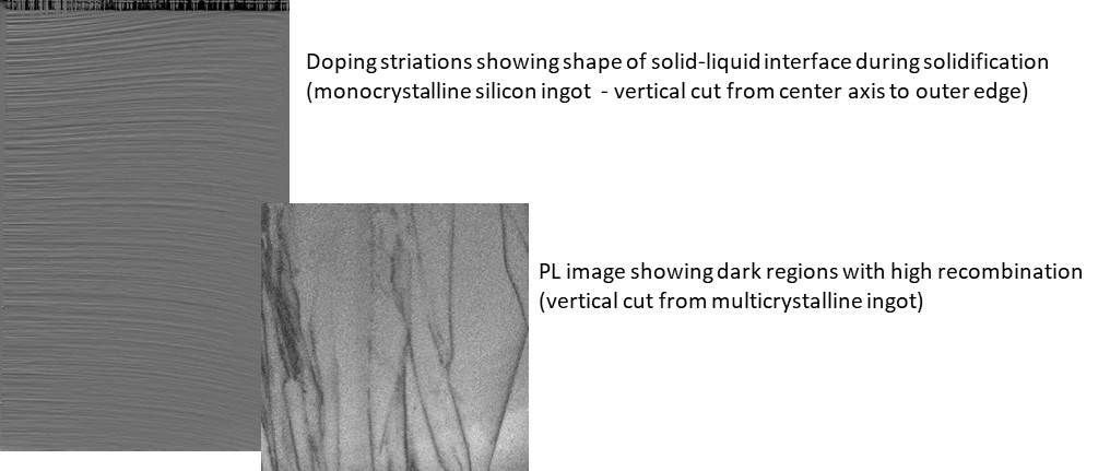 lting current is detected as a voltage drop between the two opposite contacts at the rims of the sample. The magnitude of the measured voltage depends on the lateral resistivity gradient. The technique is used to detect dopant and oxygen striations in silicon. From the striation profiles it is possible to detect the shape of the solid-liquid interface during solidification and how the interface shape changes during solidification.
In PL imaging, photolumenscence will be emitted when electron-hole pairs generated by the laser relax back to their original state (i.e. recombine). The PL intensity is measured and provides information about the silicon quality where regions with high recombination are shown as dark areas in the PL image. Dark areas are related to regions with a high defect density, typically caused by dislocations or grain boundaries decorated with impurities. The measurements are only qualitative and do not provide minority carrier lifetime values.
Striations in as-cut silicon samples are hardly visible and it is recommended that the sample surface is polished before LPS measurement. PL requires polished surface.
Published by Rannveig Kvande, SINTEF