| Time |
Title |
Speakers |
| 10:30 |
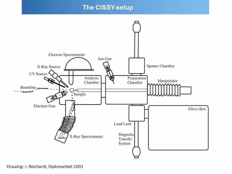
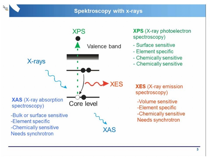
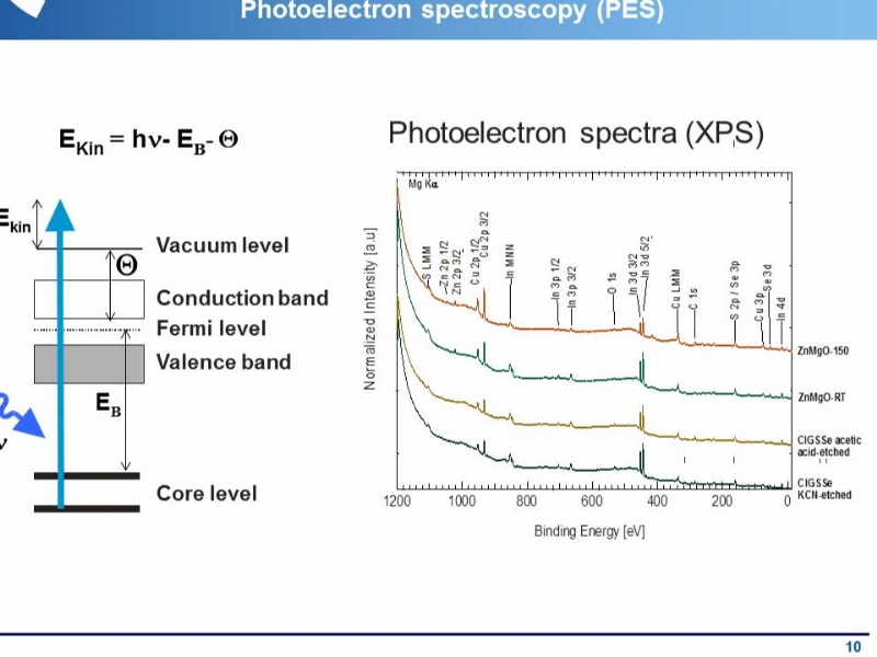
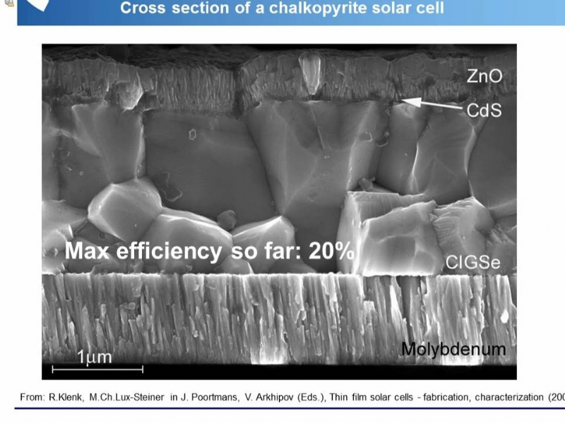
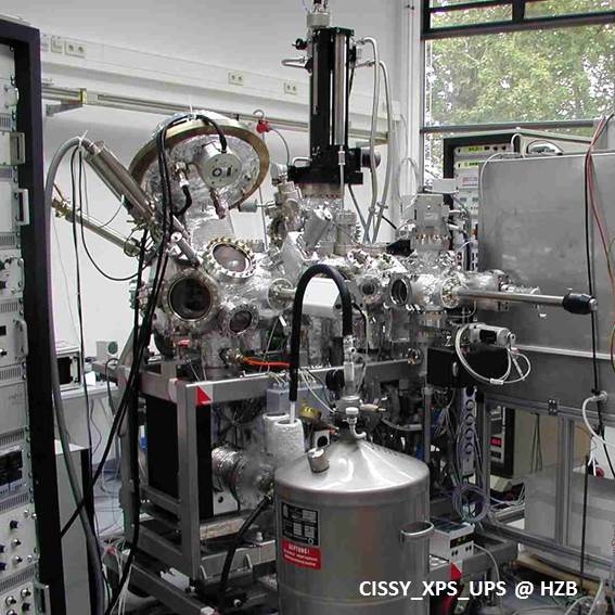
X-ray based analysis of PV materials and components |
 LAUERMANN Iver
|
The use of x-ray based spectroscopy like x-ray photoemission, x-ray absorption and x-ray emission spectroscopy for the characterization of materials and components used in photovoltaic devices is described. The emphasis is on thin film materials like chalcopyrites, kesterites, perovskites and TCO. Examples will be given on the chemical analysis of surfaces and interfaces of these materials and on the determination of electronic properties like work functions and band offsets.
|
| 10:40 |
Measurements under concentrated light |
 SCHMID Martina
|
We present two measurement setups for characterization under concentrated light (1-100 suns): 1) based on a xenon lamp providing a AAA AM1.5 spectrum for recording of jV curves, 2) utilizing a supercontinuum laser for jV and EQE measurements. These setups will be open for measurements shortly
|
| 10:50 |
EBIC & PL for thin film solar cell characterization |
 BISSING Benjamin
|
Electron beam induced current and time resolved photoluminescence technique for thin film solar cell characterization
The electron beam induced current (EBIC) and time resolved photoluminescence (TRPL) techniques are discussed as tools for determination of minority carrier metrics (decay kinetics, diffusion length) in polycrystalline thin film absorbers. Effects of injection levels, energies and sample state are discussed and general considerations for artefact reduction are presented.
|
| 11:10 |
Characterization of intermediate band materials and solar cells |
 DEL CAÑIZO Carlos
|
The main capabilities of the Intermediate Band Materials and Solar Cells Characterization Laboratory run by the Instituto de Energia Solar will be described, with emphasis in advanced optoelectronic characterisation techniques, including photomodulated reflectance, DLTS, Hall, FTIR... and current-voltage and quantum efficiency measurements that can be performed at low” “temperatures (until 7 K). Some representative measurements on intermediate band materials and solar cells will be presented and analysed.
|
| 11:30 |
Photoluminescence and Raman spectroscopy for defect identification in Silicon, CIGS and CZTS thin films |
 BINETTI Simona
|
In this presentation the potentiality of using PL and Raman spectroscopy for defect identifications in PV materials will be discussed. The advantages of using these tools in optimization of a growth process will be presented with some examples of our recent results.
|
| 11:50 |
Characterization of oxygen-related defects in high-efficiency Czochralski silicon wafers |
 VEIRMAN Jordi
|
Oxygen is by far the most abundant impurity in nowadays monocrystalline silicon wafers obtained by the Czochralski process. If harmful as such, Oxygen can however form a plurality of defects during ingot/cell processing, leading to unacceptably large efficiency drops at the solar cell level (up to 4% absolute). As ever higher efficiencies are targeted, the Oxygen content as well as the concentration of the related defects (precipitates, boron-oxygen complexes, thermal donors etc) have to be accurately measured. This is required for instance for quality control purposes, or pulling/cell process optimization. However current non-destructive techniques such as FTIR are not easy transferable to thin as-cut wafers, and do not provide a global picture of oxygen-related populations. In this context, we developed a technique named Oxymap together with AET Technologies (France), based on contactless resistivity measurements and appropriate wafer anneals, which has proven non-destructive and independent of surface state and thickness. We present an overview of the latest results obtained on large measurement volumes, in the frame of the technique developments.
|
| 12:10 |
PV Material Discussion and Idea Generation Forum |
|
|
|
| 13:00 |
Characterization of organic solar cells: Mechanical, electrical and photovoltaic stability |
 CORAZZA Michael
|
The talk covers the topic of stability characterization of interfaces in organic photovoltaic devices. Alterations of mechanical properties at the interfaces of organic solar cells during exposure to different ageing conditions and the investigation of electrical properties of the cells using impedance spectroscopy in combination with ISOS ageing tests will be discussed. The talk will be concluded with short overview of useful techniques for characterizing the interfaces of organic solar cells.
|
| 13:20 |
Advanced material and device characterization techniques for Silicon and thin-film based photovoltaics |
 GORDON Ivan
|
In this presentation, we review some advanced characterization techniques used at IMEC to study absorber materials and solar cells and modules. For material characterization, we will focus on techniques such as photoluminescence-based measurements for extracting the lifetime of silicon wafers as well as thin-film absorbers such as kesterites. For device characterization, we will focus on techniques such as dynamic local illumination to study the effect of (short) local light inhomogeneities (such as caused by clouds) on the performance of PV modules
|
| 13:40 |
Identification of degradation and manufacturing issues using multi-parameter mapping of organic solar cells |
 CASTRO Fernando Araujo de
|
The key issues hindering adoption of organic solar cells are lifetime and upscaling of production with minimal quality loss. The talk will show how a combination of advanced mapping methods can be used to identify degradation mechanisms and quality of manufacturing of organic solar cells. Results of measurements under simulated environmental degradation will also be shown and discussed.
|
| 14:20 |
Solar Cell Discussion |
|
|
|
| 14;00 |
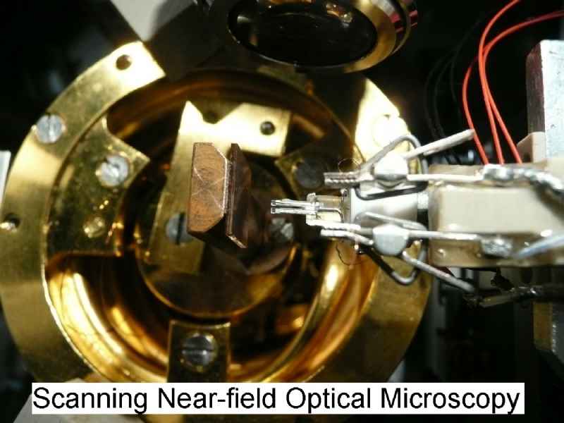
Electro-optical Characterization of Thin-film Solar Cells and Modules: From nanophotonic cell characterization to macroscopic module characterization |
 BITTKAU Karsten
|
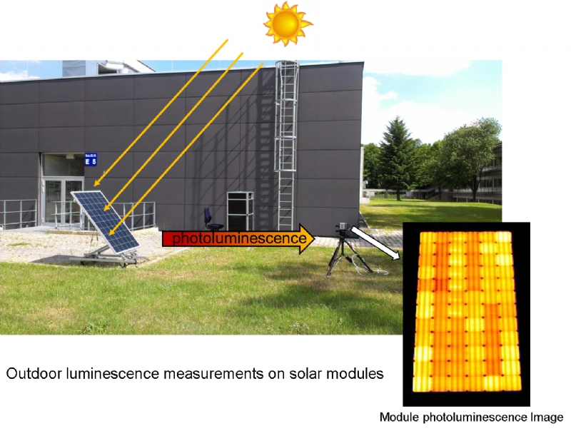
Electro-optical characterization is of significant importance along the process chain of thin-film solar cell and module fabrication on nanoscopic, as well as on a macroscopic scale. On the nano-scale, scanning near-field optical microscopy is a versatile tool to characterize the optical behavior of nano-photonic surface elements for light management. This can be done either with one probe and global illumination, two probes to investigate the light propagation within the solar cell on a microscopic range, as well as combined with a measurement of local photocurrent (nano LBIC). On the macroscopic range, such thin-film cells are interconnected to modules. A combination of electroluminescence (EL) and dark lock-in infrared thermography (DLIT) assisted by an integrated circle device simulation allows to determine local cell characteristics and advanced characterization of the modules.
|
| 15:10 |
Analytical prediction of photovoltaic modules efficiency for different encapsulation schemes |
 MACHADO Maider
|
A simple analytical calculation which allows the prediction of photovoltaic (PV) module efficiencies in different encapsulation conditions from a reduced set of experimental measurements of a reference encapsulation scheme will be presented. This procedure avoids the need to manufacture and characterize by solar simulator or External Quantum Efficiency measurements all the variety of PV modules of interest at research or manufacturing level. The absorptivity of solar cells once encapsulated is not directly accessible from direct air- bare cell or air - encapsulated cell optical measurements, and analytical or numerical methods are generally needed. This calculation is based on an optical method for multilayer glazing systems which provides analytical expressions for the layer-by-layer absorption of the different components of a PV module. From a small set of experimental measurements and the calculated spectral absorptivity values, the short-circuit current of a module can be predicted for any encapsulation scheme. It will be proved that the method accurately matches short-circuit current density and spectral External Quantum Efficiency values of the module as obtained from experimental measurements. Results will be presented for silicon and CIGS cell technologies with several glass and encapsulation materials combinations.
|
| 15:50 |
Precision PV Performance Assessment at the JRC's European Solar Test Installation |
 TAYLOR Nigel
|
The ESTI laboratory is a focal point for research on PV performance assessment. It provides reference measurements for EU research projects, laboratories and industry; it organises training events to promote best practices; it coordinates interlaboratory comparisons and contributes to collaborative R&D projects. ESTI is open to proposals for hosting visiting scientists and technicians to exploit its unique facilities, which include a range of solar simulators for cells and modulus as well as an outdoor calibration platform. The presentation will address briefly 3 areas: firstly, new developments that can half the uncertainty in measurement of power of PV devices; secondly, measurement of multijunction flat plate modules and thirdly, the proposed IEC energy rating standard
|
| 15:50 |
Degradation and electric behavior in thin film photovoltaic devices |
RENNHOFER Marcus
|
Behavior of thin film photovoltaic devices is different considering operation in the field and measurement in the lab. In the latter especially the reproducible and harmonized measurement of the output power (power rating) in the laboratory is an unsolved problem. Not only new technologies, also well-established technologies like CdTe and CIGS cannot be measured stable and reproducible without huge effort due to intrinsic metastable electric behavior under any kind of illumination. The presented study shows the correlation of this metastable behavior to the device quality for the CdTe and CIGS technology.
|
| 16:10 |
Accurate yearly yield calculation using PV module fingerprint method applied for MWT, H-pattern and thin film modules |
 KROON Jan
|
A simple and accurate method will be presented to determine the yearly yield of a module in kWh/kWp for x-Si (MWT back contact and H-pattern) and thin film modules based on the fingerprint of a module. The input for the fingerprint is the irradiance, ambient and module temperature and power output of the module recorded outdoors during a limited timeframe. The accuracy of the method was determined by comparing the calculated yield with actual measured yield.
|
| 16:30 |
CRES PV labs and outdoor long term energy yield measurements and performance evaluation |
 TSELEPIS Stathis
|
The department of PVs and Distributed Generation, located at CRES premises in Athens is equipped with facilities and laboratories which cover a wide range of applications and research studies in the field of Photovoltaics and Distributed Energy Resources. The basic laboratory equipment and test capabilities of our institution will be outlined. These laboratories are equipped with all necessary 'tools' in order to cover a wide range of research activities and also offer services to companies, organizations or private citizens which are interested in evaluating a system like a PV module or inverter.
During the presentation energy yield measurement and performance evaluation of two PV module technologies were presented.
|
| 16:40 |
Solar Systems Discussion and Idea Generation Forum |
|
|
|